Brand
:
Pololu
Product Code
:
18241
Ölçüm Parametresi
:
Mesafe Ölçüm Aralığı
:
400cm Çalışma Voltajı
:
2.6-5.5V/DC 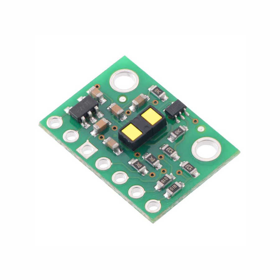


Out Of Stock
Notify me when its in stock
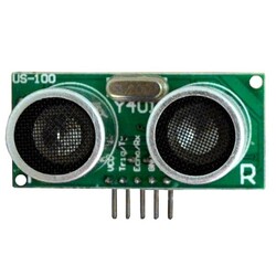
VL53L1X Time-of-Flight Distance Sensor
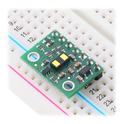
This sensor is a carrier/breakout board for ST’s VL53L1X laser ranging sensor and offers fast and accurate distance measurement up to 4 meters. Using the time-of-flight (ToF) of invisible, eye-safe laser pulses, it measures absolute distances independently of ambient lighting conditions and target characteristics such as color, shape, and texture. The VL53L1X also has a programmable region of interest (ROI), allowing the full field of view to be reduced or divided into multiple zones. Distance measurements can be read through the digital I²C interface. The board includes a 2.8 V linear regulator and level shifters; this allows devices with an input voltage range of 2.6 V to 5.5 V to operate and makes it easy to use with standard solderless breadboards with 0.1″ pin spacing.
It is a board where ST Microelectronics’ VL53L1X long-range time-of-flight (TOF) sensor is integrated into a compact module.
It is recommended to carefully read the VL53L1X datasheet (1MB PDF) before using this product.
The VL53L1X is a small, self-contained lidar system that includes an effectively integrated 940 nm Class 1 laser; this laser is invisible and eye-safe.
Unlike traditional IR sensors that use the intensity of reflected light to estimate the distance to an object, the VL53L1X uses ST’s FlightSense technology to precisely measure how long it takes for emitted infrared laser light pulses to reflect back to the detector from the nearest object.
This approach provides absolute distance measurement and allows it to remain independent of ambient lighting conditions and target characteristics such as color, shape, texture, and reflectivity; however, these external conditions also affect the sensor’s maximum range, and the same applies to sensor configuration settings.
Under more suitable conditions—a highly reflective target with low ambient lighting—you can refer to the datasheet for more information about how factors such as the maximum range the sensor can report, repeatability, and ranging error are affected.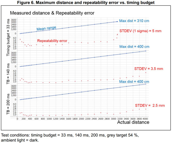
The VL53L1X offers three distance modes: short, medium, and long. Long distance mode allows the longest possible range of 4 m, but the maximum range is significantly affected by ambient light. Short distance mode is mostly unaffected by ambient light, but the maximum range is generally limited to 1.3 m (4.4 ft). The maximum sampling rate is 50 Hz in short distance mode and 30 Hz for medium and long distance modes. Performance can be improved in all modes by using lower sampling rates and longer timing budgets, as shown in the figure above.
For advanced applications, the VL53L1X supports configurable thresholds that can be used to trigger interrupts when a target is detected below a certain distance, beyond a certain distance, outside a range, or within a range. It also supports an alternative detection mode that generates an interrupt when no target is present. In addition, unlike previous models, the VL53L1X supports a configurable region of interest (ROI) within the full 16x16 detection array, allowing you to reduce the field of view (FoV). When all 256 detection elements are enabled, the FoV is 27°. A specially tuned “Autonomous Low Power” mode is available for advanced presence detection. This mode saves a significant amount of system power by automatically turning off or waking the host when a person or object is detected within the configured distance thresholds in the region of interest.
The VL53L1X is a great integrated circuit, but its small leadless LGA package makes it difficult for a typical student or hobbyist to use. It also operates at the recommended 2.8 V voltage, which can make interfacing with microcontrollers running at 3.3 V or 5 V difficult. Our breakout board addresses these issues and makes it easy to get started with the sensor while keeping the overall size as small as possible.
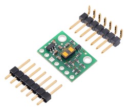
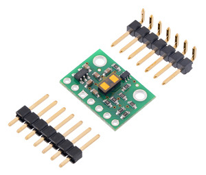
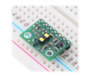
The carrier board includes a low-dropout linear voltage regulator that provides the 2.8 V required by the VL53L1X and allows the sensor to operate from a supply ranging from 2.6 V to 5.5 V. The regulator output is available on the VDD pin and can supply nearly 150 mA to external devices. The circuit board also includes a circuit that shifts the I²C clock and data lines to the same logic voltage level as the supplied VIN, making it easy to interface the board with 3.3 V or 5 V systems. The board’s 0.1″ pin spacing makes it easy to use with standard solderless breadboards and 0.1″ perfboards. The board ships fully populated with SMD components, including the VL53L1X, as shown in the product image.
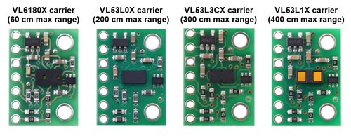
For similar but shorter-range sensors, see our 200 cm VL53L0X carrier and 60 cm VL6180X carrier. Both are physical drop-in replacements for the VL53L1X carrier, but they have different APIs, so VL53L1X software will need to be rewritten to work with the VL53L0X or VL6180X.
Features and Specifications
Included Components
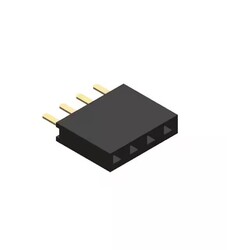
A 1×7 strip of 0.1″ header pins and a 1×7 strip of 0.1″ right-angle header pins are included, as shown in the image below. You can solder the header strip of your choice to the board for use with custom cables or solderless breadboards, or you can solder wires directly to the board itself for more compact installations.
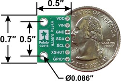
The board has two mounting holes spaced 0.5 inches apart, compatible with #2 and M2 screws (not included).
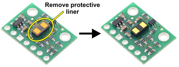
Important Note: This product may ship with a protective liner covering the sensor IC. The liner must be removed for proper sensing performance.
At least four connections are required to use the VL53L1X board: VIN, GND, SCL, and SDA. The VIN pin should be connected to a 2.6 V to 5.5 V source, and GND should be connected to 0 volts. An onboard linear voltage regulator converts VIN to a 2.8 V supply for the VL53L1X IC. Note that if your input voltage is below 3.5 V, you can connect directly to VDD instead of bypassing the regulator; in this configuration, VIN should be left disconnected. The I²C pins, SCL and SDA, are connected to onboard level shifters that make them safe to use at voltages above 2.8 V; they should be connected to an I²C bus operating at the same logic level as VIN. The XSHUT pin is an input and the GPIO1 pin is an open-drain output; both pins are pulled up to 2.8 V by the board. They are not connected to the level shifters on the board and are not 5V tolerant, but they can be used as they are with many 3.3 V and 5 V microcontrollers: the microcontroller can read the GPIO1 output as long as its logic-high threshold is below 2.8 V, and the microcontroller can drive the XSHUT pin by switching its own output between low and high-impedance states. Alternatively, our 4-channel bidirectional logic level shifter can be used externally with these pins.
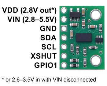
| PIN | Description |
|---|---|
| VDD |
Regulated 2.8 V output. Nearly 150 mA is available to power external components. (If you want to bypass the internal regulator, you can instead use this pin as an input for voltages between 2.6 V and 3.5 V while VIN is disconnected.)
|
| VIN |
This is the main power supply connection between 2.6 V and 5.5 V. The SCL and SDA level shifters pull the I²C lines to this level.
|
| GND |
Ground (0 V) connection for your power supply. Your I²C control source must also share a common ground with this board.
|
| SDA |
Level-shifted I²C data line: HIGH is VIN, LOW is 0 V
|
| SCL | Level-shifted I²C clock line: HIGH is VIN, LOW is 0 V |
| XSHUT |
This pin is an active-low shutdown input; the board pulls it up to VDD to enable the sensor by default. Pulling this pin low puts the sensor into hardware standby mode. This input is not level-shifted.
|
| GPIO1 |
Programmable interrupt output (VDD logic level). This output is not level-shifted.
|
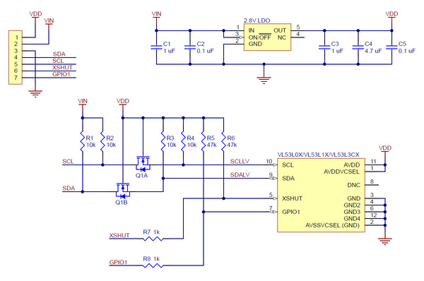
The schematic above shows the additional components included on the carrier board to make the VL53L1 easy to use, including the voltage regulator that allows the board to be powered from a 2.6 V to 5.5 V supply and the level-shifting circuit that allows I²C communication at the same logic voltage level as VIN. This schematic is also available as a downloadable PDF (110k PDF).
I²C Communication
The VL53L1X can be configured and distance readings can be queried over the I²C bus. Level shifters on the I²C clock (SCL) and data (SDA) lines allow I²C communication with microcontrollers operating at the same voltage as VIN (2.6 V to 5.5 V). A detailed description of the I²C interface on the VL53L1X can be found in the datasheet (1MB PDF), and more detailed information about I²C in general can be found in NXP’s I²C-bus specification (1MB PDF). The sensor’s 7-bit slave address defaults to 0101001b at power-up. It can be changed to any other value by writing to one of the device configuration registers, but the new address remains valid only until the sensor is reset or powered off. ST provides an application note (196k PDF) explaining how to use multiple VL53L0X sensors on the same I²C bus by bringing each sensor out of reset one at a time and assigning it a unique address, and the approach can easily be adapted to apply to the VL53L1X instead. The I²C interface on the VL53L1X is compatible with the I²C fast mode (400 kHz) standard. In our tests on the board, we were able to communicate with the chip at clock frequencies up to 400 kHz; higher frequencies may work but have not been tested.
Unlike the information available for many other devices, ST has not publicly released a register map, descriptions, or other documentation related to configuring and controlling the VL53L1X. Instead, communication with the sensor is intended to be handled through ST’s VL53L1X API (STSW-IMG007), which is a set of C functions that handle the low-level interface. To use the VL53L1X, you can customize the API to run on your chosen host platform using the information in the API documentation. Alternatively, it is also possible to use the API source code as a guide for your own implementation.
Simple Code
For the VL53L1X, we wrote a basic library that can be used as an alternative to ST’s official API for interfacing this sensor with Arduino® boards or an Arduino®-compatible controller. The library makes it easy to configure the VL53L1X and read distance data via I²C. It also includes example sketches showing how to use the library. We also have an implementation of ST’s VL53L1X API for Arduino, including an example sketch. Compared to our library, the API has a more complex interface and uses more storage and memory, but it offers some advanced functions that our library does not provide and has more robust error checking. Consider using the API for advanced applications, especially where storage and memory are less of an issue.
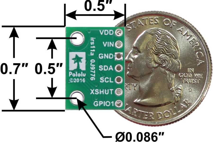
Dimensions:
| Size: | 0.5″ × 0.7″ × 0.085″1 |
|---|---|
| Weight: | 0.5 g1 |
| Resolution | 1 mm |
|---|---|
| Maximum Distance | 400 cm2 |
| Minimum Distance | 4 cm3 |
| Interface | I²C |
| Minimum Operating Voltage | 2.6 V |
| Maximum Operating Voltage | 5.5 V |
| Supply Current | 15 mA4 |
Identifying Markings:
| PCB dev codes: | irs11a |
|---|---|
| Other markings: | 0J9776 |